16:05
CST Tutorial: CST Microstrip Patch Antenna Design & Simulation- 2.4 GHz
Tensorbundle
Overview
This video provides a step-by-step guide to designing and simulating a 2.4 GHz microstrip patch antenna using CST Studio Suite. It covers the initial project setup, defining substrate and ground plane dimensions, drawing the radiating patch and microstrip feed line, and implementing an inset for impedance matching. The tutorial concludes with setting up the simulation, running it, and interpreting key results like S11 (return loss) and directivity to verify antenna performance.
How was this?
Save this permanently with flashcards, quizzes, and AI chat
Chapters
- Launch CST Studio Suite and select 'Antennas' and 'Planar' templates.
- Choose the 'Time Domain' solver for simulation.
- Define the frequency range from 2.2 GHz to 2.6 GHz for analysis.
- Set up monitors for electric field (at 2.4 GHz), magnetic field (for surface current), and far-field (for radiation pattern).
Proper project setup ensures the simulation environment is configured correctly to accurately model and analyze the antenna's behavior within the desired frequency band.
Setting the minimum frequency to 2.2 GHz and maximum frequency to 2.6 GHz, with an electric field monitor at 2.4 GHz.
- Define the substrate dimensions: length (along V-axis), width (along U-axis), and thickness (along W-axis).
- Assign the substrate material as FR4 with a permittivity of 4.3.
- Draw the ground plane with dimensions matching the substrate, using copper for the material and a thickness of 0.35 mm.
The substrate's dielectric properties and dimensions, along with the ground plane, form the foundation of the antenna and significantly influence its electrical performance and resonant frequency.
Substrate dimensions: Length (SL) = 59 mm, Width (SW) = 76 mm, Thickness (SH) = 1.5 mm. Ground plane dimensions match these, using copper with 0.35 mm thickness.
- Position the local coordinate system on top of the substrate.
- Draw the radiating patch with defined length (PL) and width (PW).
- Use copper material with a thickness of 0.35 mm for the patch.
The patch is the primary radiating element; its dimensions directly determine the antenna's resonant frequency and radiation characteristics.
Patch dimensions: Length (PL) = 29.5 mm, Width (PW) = 38 mm, using copper with 0.35 mm thickness.
- Create a microstrip line connected to the patch for feeding the signal.
- Calculate the feed line length (ML) based on substrate and patch dimensions to achieve a 50-ohm impedance.
- Implement an inset cut into the patch to fine-tune impedance matching, using a trial-and-error or calculated approach.
The feed line delivers the RF signal to the patch, and the inset is crucial for matching the antenna's impedance to the source (e.g., 50 ohms), minimizing signal reflection and maximizing power transfer.
Microstrip line width is 2.86 mm. Inset length (INL) is 9 mm and width (INW) is 74 mm, with the cut made on the negative V-axis.
- Define a waveguide port at the feed line to excite the antenna.
- Calculate the port extension coefficient (K) and use it to determine the port dimensions.
- Configure the solver settings: normalize to 50 ohms and enable adaptive mesh refinement.
- Save the project before running the simulation.
The port defines the input/output point for the electromagnetic wave, and correct solver settings ensure an accurate and efficient simulation process.
Calculating K = 5.62 and using it to define the waveguide port size relative to the substrate thickness (SH).
- Execute the simulation using the configured solver settings.
- Analyze the S11 (return loss) plot to find the resonant frequency and bandwidth.
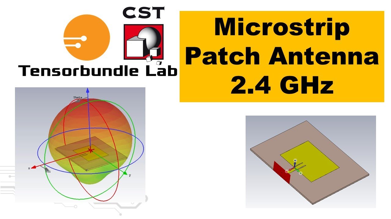
- Examine the directivity plot to understand the antenna's radiation pattern and gain.
- Interpret the surface current distribution to visualize current flow on the antenna.
Simulation results validate the antenna design by showing its performance metrics, such as how well it transmits and receives signals at the desired frequency and in which direction it radiates.
Observed resonance frequency around 2.37 GHz with S11 below -45 dB. Bandwidth is approximately 2.34 GHz to 2.41 GHz. Directivity is 6.9 dBi, with maximum radiation at the top of the patch.
Key takeaways
- Antenna design in CST involves setting up the project, defining geometric and material properties, and configuring simulation parameters.
- The dimensions of the patch and ground plane are critical for determining the antenna's resonant frequency.
- Impedance matching, achieved through techniques like inset feeding, is essential for efficient power transfer between the source and the antenna.
- The waveguide port setup is vital for accurately exciting the antenna model during simulation.
- S11 (return loss) indicates how well the antenna is matched to the transmission line; lower values (more negative) are better.
- Directivity quantifies the antenna's ability to focus radiated power in a specific direction.
- Adaptive mesh refinement can improve simulation accuracy but increases computation time.
Key terms
Microstrip Patch AntennaCST Studio SuiteTime Domain SolverSubstratePermittivity (εr)Ground PlaneRadiating PatchMicrostrip LineInset FeedImpedance MatchingWaveguide PortS11 (Return Loss)Resonant FrequencyBandwidthDirectivityAdaptive Mesh Refinement
Test your understanding
- What are the essential components of a microstrip patch antenna design in CST, and how are they defined?
- Why is impedance matching important for antenna performance, and what technique is used in this tutorial?
- How do the dimensions of the radiating patch and substrate affect the antenna's resonant frequency?
- What do the S11 and directivity results tell us about the performance of the simulated antenna?
- How does the setup of the waveguide port influence the simulation accuracy?