1:24:35
E86 Lecture 21
Prof. Dato
Overview
This lecture explores the electrical and optical properties of materials, focusing on semiconductors. It explains how materials can be processed to alter their electrical conductivity, introducing concepts like electrons, holes, intrinsic and extrinsic semiconductors, and PN junctions. The lecture also delves into how a material's band gap influences its optical properties, determining transparency, translucency, and opacity. Finally, it combines these concepts to explain the functioning of light-emitting diodes (LEDs), highlighting the importance of material processing for electronic device performance.
How was this?
Save this permanently with flashcards, quizzes, and AI chat
Chapters
- Materials can be processed to change their electrical properties, affecting how electronic components function.
- The band gap of a material determines its optical properties, influencing transparency, translucency, and opacity.
- Metals have overlapping or no band gaps, allowing free electron movement and making them opaque.
- Ceramics and polymers have large band gaps (greater than 2 eV), making them electrical insulators and potentially transparent.
- Semiconductors have small band gaps, similar to insulators but with less energy required to excite electrons.
Understanding the fundamental band structures of different material classes is crucial for predicting and manipulating their electrical and optical behaviors, which underpins the design of all electronic devices.
Metals have a band structure with filled and empty states in the same band, allowing easy electron movement, while ceramics and polymers have a large energy gap between a filled valence band and an empty conduction band.
- In semiconductors, energy input can excite an electron from the valence band to the conduction band, creating a free electron and a vacant state called a 'hole'.
- Both electrons (negative charge) and holes (positive charge) can move and act as charge carriers.
- Holes move when a nearby electron fills the vacant state, effectively causing the hole to shift in the opposite direction of electron movement.
- The electrical conductivity of a semiconductor depends on the concentration and mobility of both electrons and holes.
Identifying and understanding the behavior of electrons and holes as charge carriers is fundamental to comprehending how semiconductors conduct electricity and form the basis of electronic circuits.
When an electron in a silicon atom's covalent bond is excited, it leaves behind a hole; under an electric field, another valence electron moves to fill this hole, causing the hole to appear to move to the left.
- Intrinsic semiconductors are pure materials (like silicon or germanium) whose electrical properties are inherent.
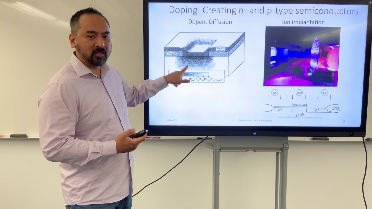
- Extrinsic semiconductors are created by doping, which involves intentionally adding impurity atoms to alter electrical properties.
- Doping with Group 5 elements (e.g., phosphorus) creates n-type semiconductors, introducing extra electrons (donor states) that easily move to the conduction band.
- Doping with Group 3 elements (e.g., boron) creates p-type semiconductors, introducing 'holes' (acceptor states) that readily accept electrons from the valence band.
Doping allows precise control over a semiconductor's conductivity, enabling the creation of n-type and p-type materials essential for building complex electronic components like diodes and transistors.
Adding phosphorus (a Group 5 element) to silicon (a Group 4 element) results in an n-type semiconductor because the extra valence electron from phosphorus occupies a donor state just below the conduction band, requiring little energy to become a free electron.
- A PN junction is formed by joining n-type and p-type semiconductor materials.
- At the junction, diffusion of electrons and holes creates a depletion region with a built-in electric field.
- Forward bias (positive voltage to p-type, negative to n-type) reduces the depletion region and allows current to flow.
- Reverse bias (positive voltage to n-type, negative to p-type) widens the depletion region and blocks current flow.
- PN junctions act as diodes, allowing current to flow primarily in one direction.
The behavior of PN junctions under different electrical biases is the fundamental principle behind diodes, transistors, and integrated circuits, enabling rectification and amplification of electrical signals.
When a positive terminal of a battery is connected to the p-type side and the negative terminal to the n-type side (forward bias), holes are pushed towards the junction from the p-side and electrons from the n-side, allowing significant current flow.
- Integrated circuits (chips) are built using microfabrication processes on silicon wafers.
- MOSFETs (Metal-Oxide-Semiconductor Field-Effect Transistors) are key components in modern chips, acting as electronic switches.
- A gate voltage controls the conductivity between the source and drain regions of a MOSFET.
- Modern transistors are incredibly small, with dimensions smaller than viruses, enabling billions to be packed onto a single chip.
- The ability to switch transistors on and off billions of times per second is the basis of digital computation (1s and 0s).
Understanding the fabrication of transistors like MOSFETs reveals the intricate engineering required to create the powerful microprocessors that drive our electronic devices, from smartphones to supercomputers.
A MOSFET can be turned 'on' by applying a negative voltage to its gate, allowing charge carriers (holes in this specific example) to flow from the source to the drain, and turned 'off' by removing that voltage.
- The energy of a photon is directly related to its frequency and inversely related to its wavelength.
- Visible light spans a photon energy range from 1.8 eV (red) to 3.1 eV (violet).
- Materials with band gaps larger than 3.1 eV are transparent and colorless because visible light photons lack the energy to excite electrons across the gap.
- Materials with band gaps between 1.8 eV and 3.1 eV absorb some visible light, appearing colored.
- Materials with band gaps less than 1.8 eV absorb all visible light, making them opaque.
The band gap is the critical factor determining whether a material interacts with visible light by absorbing, transmitting, or reflecting it, explaining why we see metals as opaque and glass as transparent.
Ceramics and polymers, having band gaps greater than 3.1 eV, do not absorb visible light photons, allowing them to pass through and making these materials appear transparent, like window glass.
- Impurities can be added to materials to create specific optical properties, such as color, by introducing energy levels within the band gap.
- Sapphire (pure aluminum oxide) is transparent, but adding chromium impurities creates ruby, which absorbs blue/green light and appears red.
- Light-Emitting Diodes (LEDs) are PN junctions that convert electrical energy into light through electron-hole recombination.
- The color of light emitted by an LED is determined by the band gap of the semiconductor material used.
- LEDs are more efficient, generate less heat, and have longer lifetimes than traditional incandescent light bulbs.
Understanding how impurities affect optical properties and how PN junctions emit light allows for the design of colored materials and efficient lighting technologies like LEDs.
In an LED, when an electron from the n-type side recombines with a hole from the p-type side, the energy released is emitted as a photon of visible light, with the color corresponding to the semiconductor's band gap.
Key takeaways
- Semiconductor properties can be precisely tuned by introducing impurities (doping) to create n-type (excess electrons) and p-type (excess holes) materials.
- The PN junction, formed by joining n-type and p-type semiconductors, is the fundamental building block for diodes and transistors, enabling directional current flow.
- The band gap of a material dictates its interaction with light: large band gaps lead to transparency, intermediate band gaps lead to color, and small band gaps lead to opacity.
- Modern electronic devices rely on billions of microscopic transistors (like MOSFETs) fabricated through complex processes, acting as high-speed switches.
- The color of an LED is directly determined by the band gap of the semiconductor material used, as electron-hole recombination releases photons of specific energies.
- Understanding material properties at the atomic and electronic level is crucial for designing advanced electronic and optical devices.
Key terms
Band GapElectronHoleIntrinsic SemiconductorExtrinsic SemiconductorDopingN-type SemiconductorP-type SemiconductorPN JunctionForward BiasReverse BiasMOSFETPhotonTransparencyOpacityLight-Emitting Diode (LED)
Test your understanding
- How does doping a semiconductor with Group 5 elements fundamentally change its electrical properties compared to doping with Group 3 elements?
- Explain the mechanism by which a PN junction blocks current flow under reverse bias.
- Why are materials with band gaps greater than 3.1 eV transparent to visible light?
- How does the band gap of a semiconductor material influence the color of light emitted by an LED?
- What is the role of a MOSFET in a modern electronic chip, and how does its operation relate to digital logic (1s and 0s)?