16:19
JFET: Construction and Working Explained
ALL ABOUT ELECTRONICS
Overview
This video explains the construction and working principles of a Junction Field-Effect Transistor (JFET). It details how the channel material (n-type or p-type) and the surrounding semiconductor regions form the device. The explanation uses a tap-water analogy to illustrate how the gate voltage controls the current flow between the drain and source. The video covers the output characteristics (drain curves) for both n-channel and p-channel JFETs, describing three operating regions: ohmic, saturation, and cut-off, as well as the breakdown region. Finally, it shows the electronic symbols for n-channel and p-channel JFETs.
How was this?
Save this permanently with flashcards, quizzes, and AI chat
Chapters
- A JFET has a semiconductor channel (n-type or p-type) through which charge carriers flow.
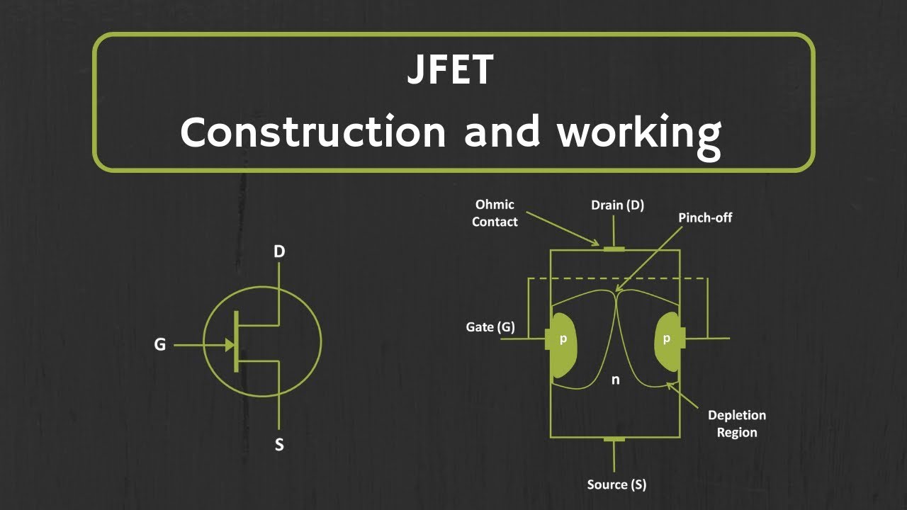
- Two small regions of the opposite semiconductor type are fabricated near the channel, forming PN junctions with it.
- The drain and source terminals are connected to the ends of the channel, while the gate terminal connects to the two opposite regions.
- The JFET's operation is analogous to a tap: the gate voltage controls the current flow (water) between the drain and source.
- In an n-channel JFET, the channel is n-type, and the gate regions are p-type. The drain-source voltage (Vds) is positive, and the gate-source voltage (Vgs) is typically negative or zero.
Understanding the physical construction and the water tap analogy helps in grasping the fundamental concept of how a voltage applied to the gate can modulate the current flow through the channel.
An n-channel JFET has an n-type channel with two p-type regions forming PN junctions. The drain is at the top, source at the bottom of the n-channel, and both p-regions are connected to the gate.
- When Vgs is zero and Vds is positive, the PN junctions become reverse-biased.
- The reverse bias creates depletion regions that widen from the gate towards the drain.
- The depletion region is wider at the drain end because the voltage drop along the channel makes the upper part of the p-type gate region more reverse-biased.
- As Vds increases, the channel resistance initially stays constant (ohmic region), then increases as depletion regions widen and narrow the channel.
- Pinch-off occurs when Vds reaches the pinch-off voltage (Vp), causing depletion regions to nearly touch, leading to current saturation (Idss).
This section explains the initial behavior of the JFET when the gate is unbiased, revealing how the channel geometry and applied drain voltage influence current flow and resistance, leading to the concept of pinch-off.
When Vds is applied to an n-channel JFET with Vgs=0, electrons flow from source to drain. The PN junctions are reverse-biased, and depletion regions form. As Vds increases, these regions widen, constricting the channel.
- Applying a negative Vgs to an n-channel JFET increases the reverse bias on the PN junctions.
- This increased reverse bias causes the depletion regions to widen further, narrowing the conductive channel.
- A more negative Vgs reduces the maximum saturation current (Idss) and shifts the pinch-off point to a lower Vds.
- When Vgs reaches the pinch-off voltage (Vp, which is negative for n-channel), the channel is completely depleted, and the drain current (Id) becomes approximately zero (cut-off region).
- The JFET can operate in three main regions: ohmic (variable resistor), saturation (constant current source), and cut-off (off).
This is crucial for understanding the JFET's primary function as a voltage-controlled device, demonstrating how the gate voltage acts as a control knob to regulate the drain current.
Decreasing Vgs from 0V to -1V, then to -2V on an n-channel JFET will progressively reduce the saturation drain current (Idss) and eventually turn the device off when Vgs reaches -Vp.
- P-channel JFETs are similar to n-channel but use a p-type channel and n-type gate regions.
- For p-channel JFETs, the drain-source voltage (Vds) is negative, and the gate-source voltage (Vgs) is typically positive or zero.
- Charge carriers in a p-channel JFET are holes, flowing from source to drain.
- The output characteristics of a p-channel JFET are similar to n-channel but mirrored on the negative voltage axis.
- The electronic symbol for an n-channel JFET has an arrow pointing inward on the gate terminal, while a p-channel JFET has an arrow pointing outward.
This section extends the understanding to the complementary p-channel JFET and provides the essential visual cues (symbols) needed to identify and differentiate JFET types in circuit diagrams.
In a p-channel JFET, the drain is typically more negative than the source, and the gate is more positive than the source. The symbol for an n-channel JFET has an inward-pointing arrow on the gate, while a p-channel has an outward-pointing arrow.
Key takeaways
- JFETs are voltage-controlled devices where the gate-source voltage modulates the conductivity of a semiconductor channel.
- The construction involves a channel and surrounding gate regions that form PN junctions, creating depletion regions that control channel width.
- The tap-water analogy effectively illustrates how the gate voltage acts as a control knob for drain current.
- JFETs exhibit distinct operating regions: ohmic (variable resistor), saturation (constant current source), and cut-off (off).
- Pinch-off is a critical condition where depletion regions nearly touch, leading to current saturation.
- N-channel and p-channel JFETs operate similarly but with reversed voltage polarities and charge carriers.
- The direction of the arrow on the gate terminal in the JFET symbol distinguishes between n-channel and p-channel types.
Key terms
Junction Field-Effect Transistor (JFET)ChannelGateDrainSourceDepletion RegionReverse BiasPinch-off Voltage (Vp)Drain Current (Id)Gate-Source Voltage (Vgs)Drain-Source Voltage (Vds)Saturation RegionOhmic RegionCut-off RegionIdss (Drain Saturation Current)
Test your understanding
- How does the width of the depletion region in a JFET change with an increasing reverse-bias voltage applied to the gate-source terminals?
- Explain the tap-water analogy and how it relates to the JFET's operation, specifically the role of the gate.
- What is the pinch-off condition in a JFET, and what happens to the drain current when this condition is reached?
- Describe the differences in construction and biasing polarities between an n-channel JFET and a p-channel JFET.
- How can the gate-source voltage (Vgs) be used to control the drain current (Id) in an n-channel JFET, and what are the three main operating regions?